Metalenz reimagines the camera in 2D and raises $10M to ship it – TechCrunch

[ad_1]
As impressive as the cameras in our smartphones are, they’re fundamentally limited by the physical necessities of lenses and sensors. Metalenz skips over that part with a camera made of a single “metasurface” that could save precious space and battery life in phones and other devices… and they’re about to ship it.
The concept is similar to, but not descended from, the “metamaterials” that gave rise to flat beam-forming radar and lidar of Lumotive and Echodyne. The idea is to take a complex 3D structure and accomplish what it does using a precisely engineered “2D” surface — not actually two-dimensional, of course, but usually a plane with features measured in microns.
In the case of a camera, the main components are of course a lens (these days it’s usually several stacked), which corrals the light, and an image sensor, which senses and measures that light. The problem faced by cameras now, particularly in smartphones, is that the lenses can’t be made much smaller without seriously affecting the clarity of the image. Likewise sensors are nearly at the limit of how much light they can work with. Consequently, most of the photography advancements of the last few years have been done on the computational side.
Using an engineered surface that does away with the need for complex optics and other camera systems has been a goal for years. Back in 2016 I wrote about a NASA project that took inspiration from moth eyes to create a 2D camera of sorts. It’s harder than it sounds, though — usable imagery has been generated in labs, but it’s not the kind of thing that you take to Apple or Samsung.
Metalenz aims to change that. The company’s tech is built on the work of Harvard’s Federico Capasso, who has been publishing on the science behind metasurfaces for years. He and Rob Devlin, who did his doctorate work in Capasso’s lab, co-founded the company to commercialize their efforts.
“Early demos were extremely inefficient,” said Devlin of the field’s first entrants. “You had light scattering all over the place, the materials and processes were non-standard, the designs weren’t able to handle the demands that a real world throws at you. Making one that works and publishing a paper on it is one thing, making 10 million and making sure they all do the same thing is another.”
Their breakthrough — if years of hard work and research can be called that — is the ability not just to make a metasurface camera that produces decent images, but to do it without exotic components or manufacturing processes.
“We’re really using all standard semiconductor processes and materials here, the exact same equipment — but with lenses instead of electronics,” said Devlin. “We can already make a million lenses a day with our foundry partners.”

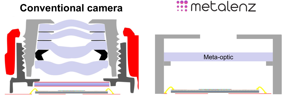
The thing at the bottom is the chip where the image processor and logic would be, but the meta-optic could also integrate with that. The top is a pinhole. Image Credits: Metalenz
The first challenge is more or less contained in the fact that incoming light, without lenses to bend and direct it, hits the metasurface in a much more chaotic way. Devlin’s own PhD work was concerned with taming this chaos.
“Light on a macro [i.e. conventional scale, not close-focusing] lens is controlled on the macro scale, you’re relying on the curvature to bend the light. There’s only so much you can do with it,” he explained. “But here you have features a thousand times smaller than a human hair, which gives us very fine control over the light that hits the lens.”
Those features, as you can see in this extreme close-up of the metasurface, are precisely tuned cylinders, “almost like little nano-scale Coke cans,” Devlin suggested. Like other metamaterials, these structures, far smaller than a visible or near-infrared light ray’s wavelength, manipulate the radiation by means that take a few years of study to understand.
The result is a camera with extremely small proportions and vastly less complexity than the compact camera stacks found in consumer and industrial devices. To be clear, Metalenz isn’t looking to replace the main camera on your iPhone — for conventional photography purposes the conventional lens and sensor are still the way to go. But there are other applications that play to the chip-style lens’s strengths.
Something like the FaceID assembly, for instance, presents an opportunity. “That module is a very complex one for the cell phone world — it’s almost like a Rube Goldberg machine,” said Devlin. Likewise the miniature lidar sensor.
At this scale, the priorities are different, and by subtracting the lens from the equation the amount of light that reaches the sensor is significantly increased. That means it can potentially be smaller in every dimension while performing better and drawing less power.

Image (of a very small test board) from a traditional camera, left, and metasurface camera, right. Beyond the vignetting it’s not really easy to tell what’s different, which is kind of the point. Image Credits: Metalenz
Lest you think this is still a lab-bound “wouldn’t it be nice if” type device, Metalenz is well on its way to commercial availability. The $10 million Series A they just raised was led by 3M Ventures, Applied Ventures LLC, Intel Capital, M Ventures and TDK Ventures, along with Tsingyuan Ventures and Braemar Energy Ventures — a lot of suppliers in there.
Unlike many other hardware startups, Metalenz isn’t starting with a short run of boutique demo devices but going big out of the gate.
“Because we’re using traditional fabrication techniques, it allows us to scale really quickly. We’re not building factories or foundries, we don’t have to raise hundreds of mils; we can use what’s already there,” said Devlin. “But it means we have to look at applications that are high volume. We need the units to be in that tens of millions range for our foundry partners to see it making sense.”
Although Devlin declined to get specific, he did say that their first partner is “active in 3D sensing” and that a consumer device, though not a phone, would be shipping with Metalenz cameras in early 2022 — and later in 2022 will see a phone-based solution shipping as well.
In other words, while Metalenz is indeed a startup just coming out of stealth and raising its A round… it already has shipments planned on the order of tens of millions. The $10 million isn’t a bridge to commercial viability but short-term cash to hire and cover upfront costs associated with such a serious endeavor. It’s doubtful anyone on that list of investors harbors any serious doubts on ROI.
The 3D sensing thing is Metalenz’s first major application, but the company is already working on others. The potential to reduce complex lab equipment to handheld electronics that can be fielded easily is one, and improving the benchtop versions of tools with more light-gathering ability or quicker operation is another.
Though a device you use may in a few years have a Metalenz component in it, it’s likely you won’t know — the phone manufacturer will probably take all the credit for the improved performance or slimmer form factor. Nevertheless, it may show up in teardowns and bills of material, at which point you’ll know this particular university spin-out has made it to the big leagues.
[ad_2]
Source link


